


1. Voltage Signal Transmission Path

As shown in Figure 1, a voltage signal transmission system consists of three key components:
Negative feedback voltage output circuit
Signal transmission cable
Includes parasitic capacitance (C1) and parasitic inductance (L1), which depend on cable length and wiring layout.
Input signal acquisition circuit
May include a low-pass filter (L2, C2).
2. Why Does Oscillation Occur?
In a negative feedback voltage signal system, the input signal is calculated as:
∣Xi′∣=∣Xi∣−∣Xf∣|X_i’| = |X_i| – |X_f|
However, if the feedback signal (|Xf|) is phase-shifted by 180°, the equation changes to:
∣Xi′∣=∣Xi∣+∣Xf∣|X_i’| = |X_i| + |X_f|
This means that even if no input signal is applied (|Xi| = 0), the feedback signal sustains the output, leading to self-sustaining oscillation.
For oscillation to occur, two conditions must be met:
Loop gain is greater than 1: |AF| > 1
Phase shift satisfies: φA + φF = (2n+1)π
The phase shift in the loop comes from multiple sources:
✔ Parasitic capacitance (C1) and inductance (L1) in the transmission cable
✔ Low-pass filter components (L2, C2) in the input circuit
✔ Filter capacitors in the output circuit
If the total phase shift reaches 180°, self-oscillation can occur.
3. How to Prevent Oscillation?
To prevent oscillation, one of the two conditions above must not be met within the operational frequency range.
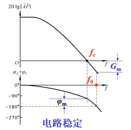
As shown in Figure 2, two critical frequencies are considered:
fc: The frequency where loop gain |AF| drops to 0 dB.
fo: The frequency where loop phase shift exceeds -180°.
To maintain stability, the gain should be below 0 dB when the phase shift reaches -180°.
4. Why Current Output Signals Are More Stable
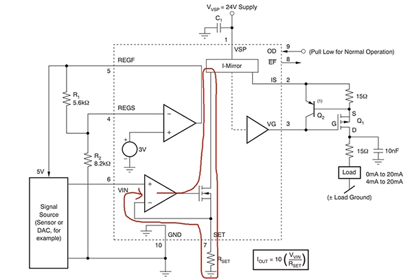
Current signal output circuits are less prone to oscillation because:
✔ Their feedback path is confined to internal components (as shown in Figure 3).
✔ External load variations have little effect on phase shift or gain.
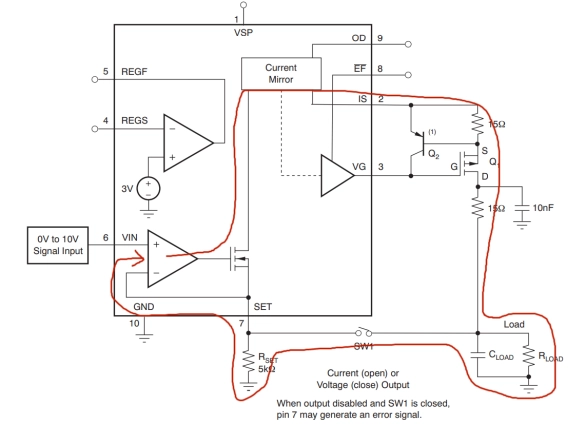
In contrast, voltage output circuits (Figure 4) take feedback from the output point, meaning that external cables and sampling circuits can influence phase shift and gain. If their parameters change, the system may meet the oscillation conditions, leading to instability.
5.Conclusion
Voltage-type output signals can oscillate when:
✔ Parasitic components introduce a 180° phase shift.
✔ Loop gain remains greater than 1 at this phase shift.
To avoid oscillation:
✔ Ensure loop gain is reduced below 0 dB before phase shift reaches 180°.
✔ Minimize parasitic capacitance/inductance in transmission cables.
✔ Use appropriate filtering to stabilize the feedback loop.
In contrast, current-type outputs are more stable since their feedback loop is less affected by external load conditions.


 鄂公网安备 42018502006527号